General Description
The RTQ2104GSP-QA evaluation board showcases the regulator’s performance, delivering 3A output from a 4V to 36V input at 2.1MHz. Suitable for industrial and communication systems, it offers protection against shorted outputs, input undervoltage, overcurrent, and thermal shutdown. The documentation includes a BOM, typical application, board overview, power-up procedure, performance summary, and hardware description to provide information on the board’s components, capabilities, and usage.
Performance Specification Summary
Summary of the RTQ2104GSP Evaluation Board performance specificiaiton is provided in Table 1. The ambient temperature is 25°C.
Table 1. RTQ2104GSP Evaluation Board Performance Specification Summary
|
Specification
|
Test Conditions
|
Min
|
Typ
|
Max
|
Unit
|
|
Input Voltage Range
|
Soft-start is finished
|
3
|
--
|
36
|
V
|
|
Output Current
|
|
0
|
--
|
3
|
A
|
|
Default Output Voltage
|
|
0.8
|
--
|
VIN
|
V
|
|
Operation Frequency
|
|
1.89
|
2.1
|
2.31
|
MHz
|
|
Output Ripple Voltage
|
VIN = 12V, VOUT = 5V, IOUT = 3A
|
--
|
10
|
--
|
mVp-p
|
|
Line Regulation
|
VOUT = 5V, IOUT = 3A, VIN = 7V to 25V
|
--
|
±1
|
--
|
%
|
|
Load Regulation
|
VIN = 12V, VOUT = 5V, IOUT = 0.5A to 3A
|
--
|
±1
|
--
|
%
|
|
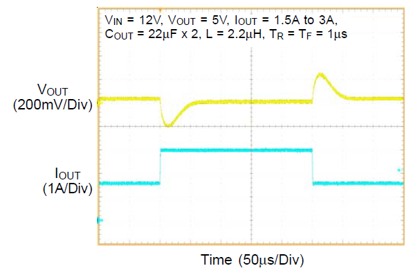
Load Transient Response
|
VIN = 12V, VOUT = 5V, IOUT = 1.5A to 3A
|
--
|
±10
|
--
|
%
|
|
Maximum Efficiency
|
VIN = 12V, VOUT = 5V, IOUT = 1.5A
|
--
|
90
|
--
|
%
|
Power-up Procedure
Suggestion Required Equipments
- RTQ2104GSP Evaluation Board
- DC power supply capable of at least 36V and 3A
- Electronic load capable of 3A
- Function Generator
- Oscilloscope
Quick Start Procedures
The Evaluation Board is fully assembled and tested. Follow the steps below to verify board operation. Do not turn on supplies until all connections are made. When measuring the output voltage ripple, care must be taken to avoid a long ground lead on the oscilloscope probe. Measure the output voltage ripple by touching the probe tip and ground ring directly across the last output capacitor.
Proper measurement equipment setup and follow the procedure below.
1) With power off, connect the input power supply to VIN and GND pins.
2) With power off, connect the electronic load between the VOUT and nearest GND pins.
3) Turn on the power supply at the input. Make sure that the input voltage does not exceeds 36V on the Evaluation Board.
4) Check for the proper output voltage using a voltmeter.
5) Once the proper output voltage is established, adjust the load within the operating ranges and observe the output voltage regulation, ripple voltage, efficiency and other performance.
Detailed Description of Hardware
Headers Description and Placement
Carefully inspect all the components used in the EVB according to the following Bill of Materials table, and then make sure all the components are undamaged and correctly installed. If there is any missing or damaged component, which may occur during transportation, please contact our distributors or e-mail us at evb_service@richtek.com.
Test Points
The EVB is provided with the test points and pin names listed in the table below.
|
Test Point/
Pin Name
|
Function
|
|
VIN
|
DC power supply positive input terminal. The input voltage range is from 3V to 36V after soft-start is finished.
|
|
VOUT
|
Electronic load positive output terminal. Draw maximum output current up to 3A.
|
|
GND
|
Reference ground for power supply or electronic load. Provide the ground return path for the control circuitry and low-side power MOSFET.
|
|
VIN_EMI+
|
Positive input terminal of EMI filter circuit.
|
|
VIN_EMI-
|
Negative input terminal of EMI filter circuit.
|
|
PG
|
Power-good indication test point. The test point can be used to measure the power-good singal.
|
|
EN
|
Enable control input. A logic-high enables the converter; a logic-low forces the device into shutdown mode.
|
|
JP1
|
EN jumper. Connect EN to logic-low to disable, connect logic-high to enable.
|
Bill of Materials
|
VIN = 12V, VOUT = 5V, IOUT = 3A, fSW = 2100kHz
|
|
Reference
|
Count
|
Part Number
|
Value
|
Description
|
Package
|
Manufacturer
|
|
U4
|
1
|
RTQ2104GSP-QA
|
RTQ2104GSP-QA
|
Step-Down Converter
|
SOP-8 (Exposed Pad)
|
RICHTEK
|
|
CFF1
|
1
|
0603B121K500CT
|
120pF
|
Capacitor, Ceramic, 50V, X7R
|
0603
|
WALSIN
|
|
CVCC1
|
1
|
GRM21BR71A106KE51L
|
10µF
|
Capacitor, Ceramic, 10V, X7R
|
0805
|
MURATA
|
|
C3
|
1
|
UMK316AB7475KL-T
|
4.7µF
|
Capacitor, Ceramic, 50V, X7R
|
1206
|
TAIYO
YUDEN
|
|
C4, C7, C16, CBOOT1
|
4
|
0603B104K500CT
|
0.1µF
|
Capacitor, Ceramic, 50V, X7R
|
0603
|
WALSIN
|
|
C5, C6
|
2
|
LMK316AB7226KL-TR
|
22µF
|
Capacitor, Ceramic, 10V, X7R
|
1206
|
TAIYO
YUDEN
|
|
R1
|
1
|
WR06X1053FTL
|
105k
|
Resistor, Chip, 1/10W, 1%
|
0603
|
WALSIN
|
|
R2
|
1
|
WR06X2002FTL
|
20k
|
Resistor, Chip, 1/10W, 1%
|
0603
|
WALSIN
|
|
RBOOT1
|
1
|
WR06X10R0FTL
|
10
|
Resistor, Chip, 1/10W, 1%
|
0603
|
WALSIN
|
|
RPG1, REN1
|
2
|
WR06X1003FTL
|
100k
|
Resistor, Chip, 1/10W, 1%
|
0603
|
WALSIN
|
|
L1
|
1
|
78439344022
|
2.2µH
|
Inductor,
Isat = 7.5A, 10.5mΩ
|
6.65x6.45x3mm
|
Würth Elektronik
|
Typical Applications
EVB Schematic Diagram
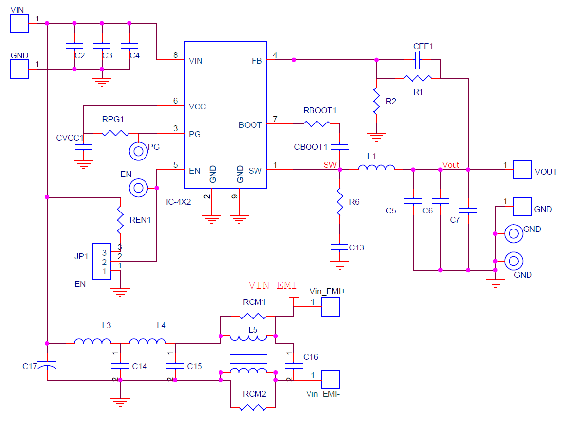
1. The capacitance values of the input and output capacitors will influence the input and output voltage ripple.
2. MLCC capacitors have degrading capacitance at DC bias voltage, and especially smaller size MLCC capacitors will have much lower capacitance.
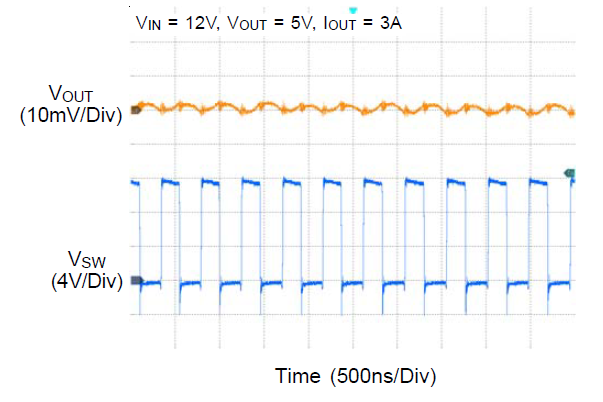
Measure Result
|
Output Ripple Measurement
|
Load Transient Response
|
|
|
|
|
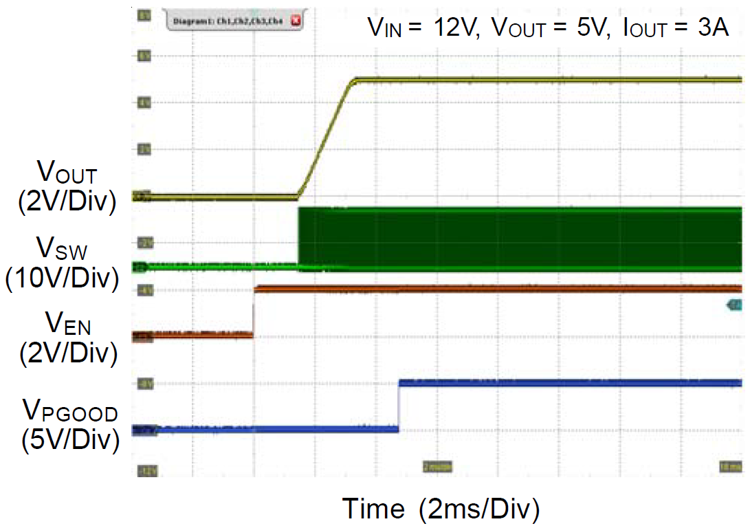
Power On from EN
|
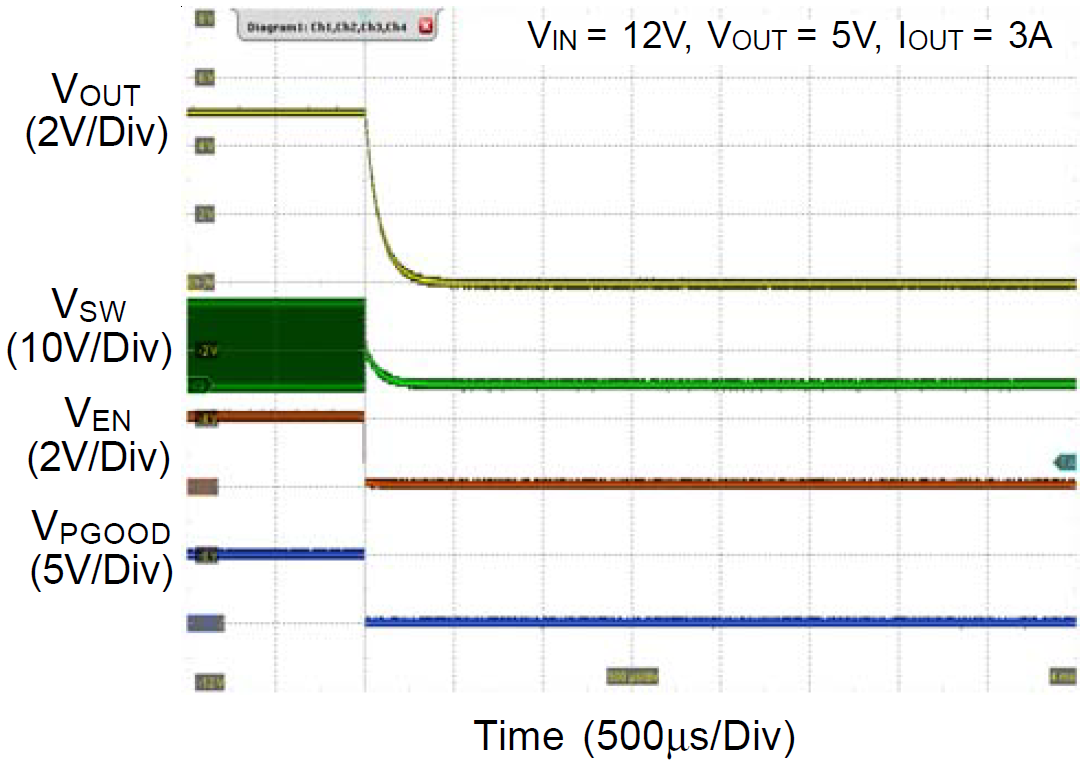
Power Off from EN
|
|
|
|
|
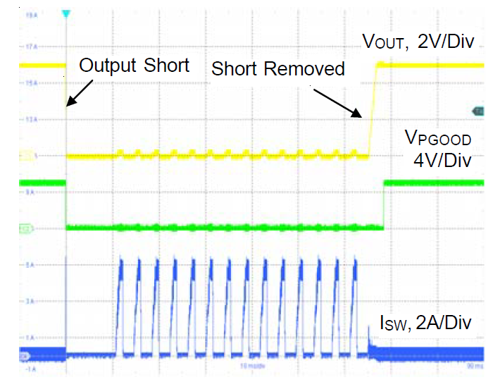
Short Circuit Response – Short and Recovery
|
Start-Up Dropout Performance
|
|
|
|
|
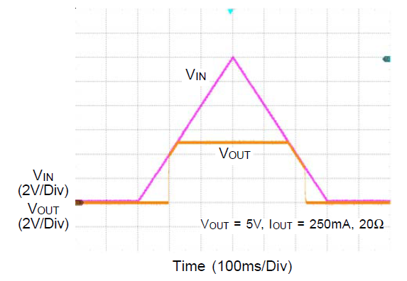
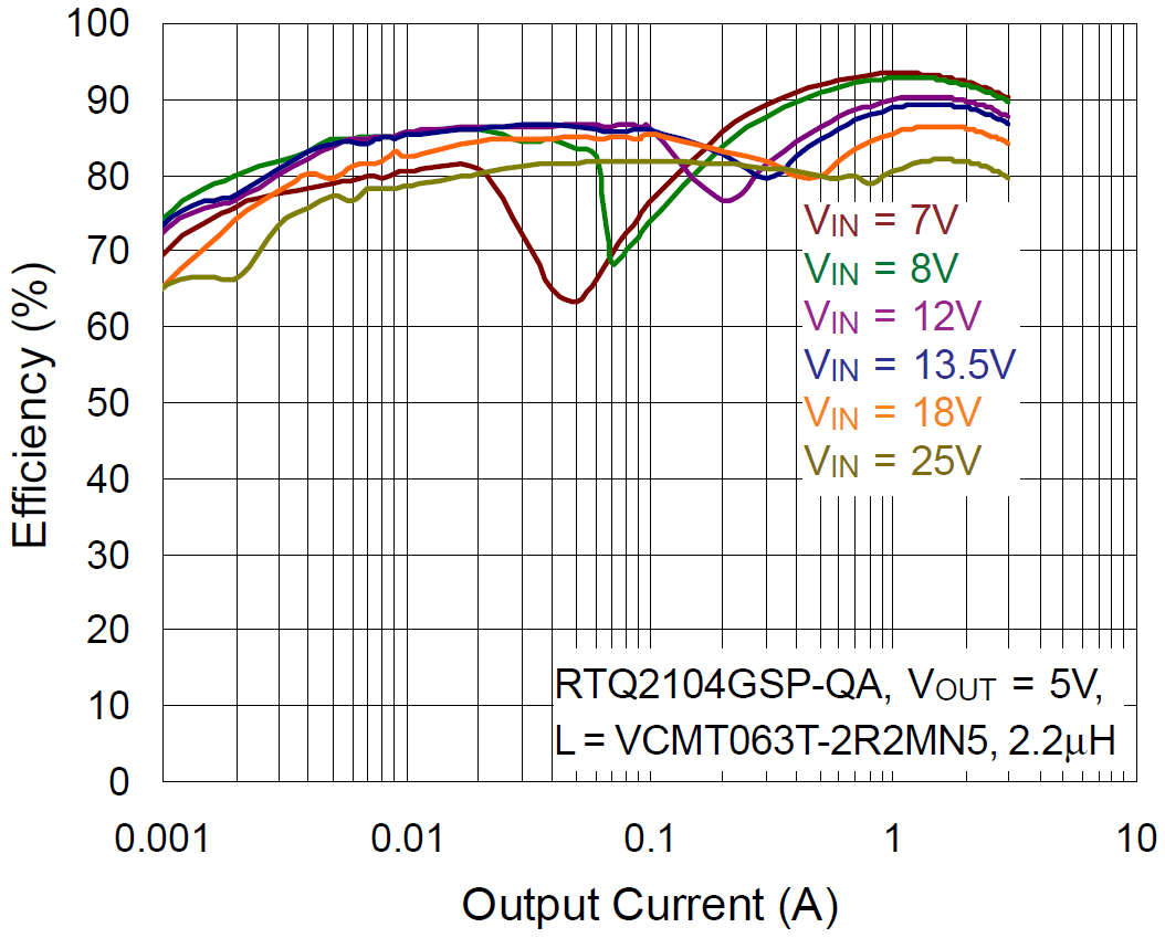
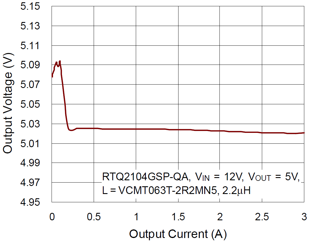
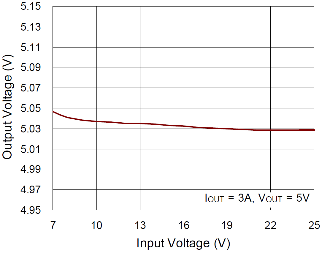
Efficiency vs. Output Current
|
Output Voltage vs. Output Current
|
|
|
|
|
Output Voltage vs. Input Voltage
|
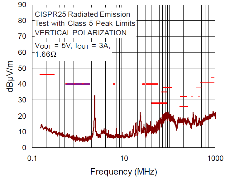
Radiated EMI Performance
|
|
|
|
Note: When measuring the input or output voltage ripple, care must be taken to avoid a long ground lead on the oscilloscope probe. Measure the output voltage ripple by touching the probe tip directly across the output capacitor.
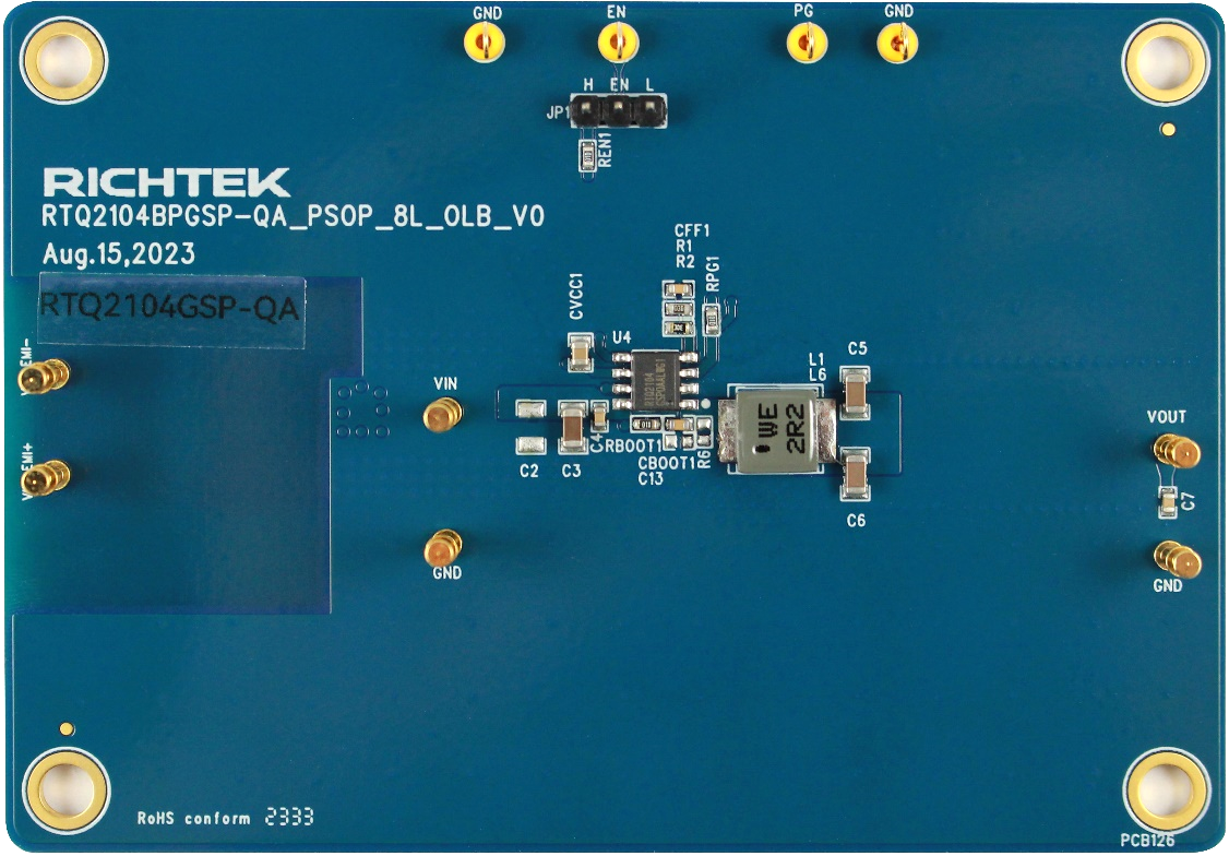
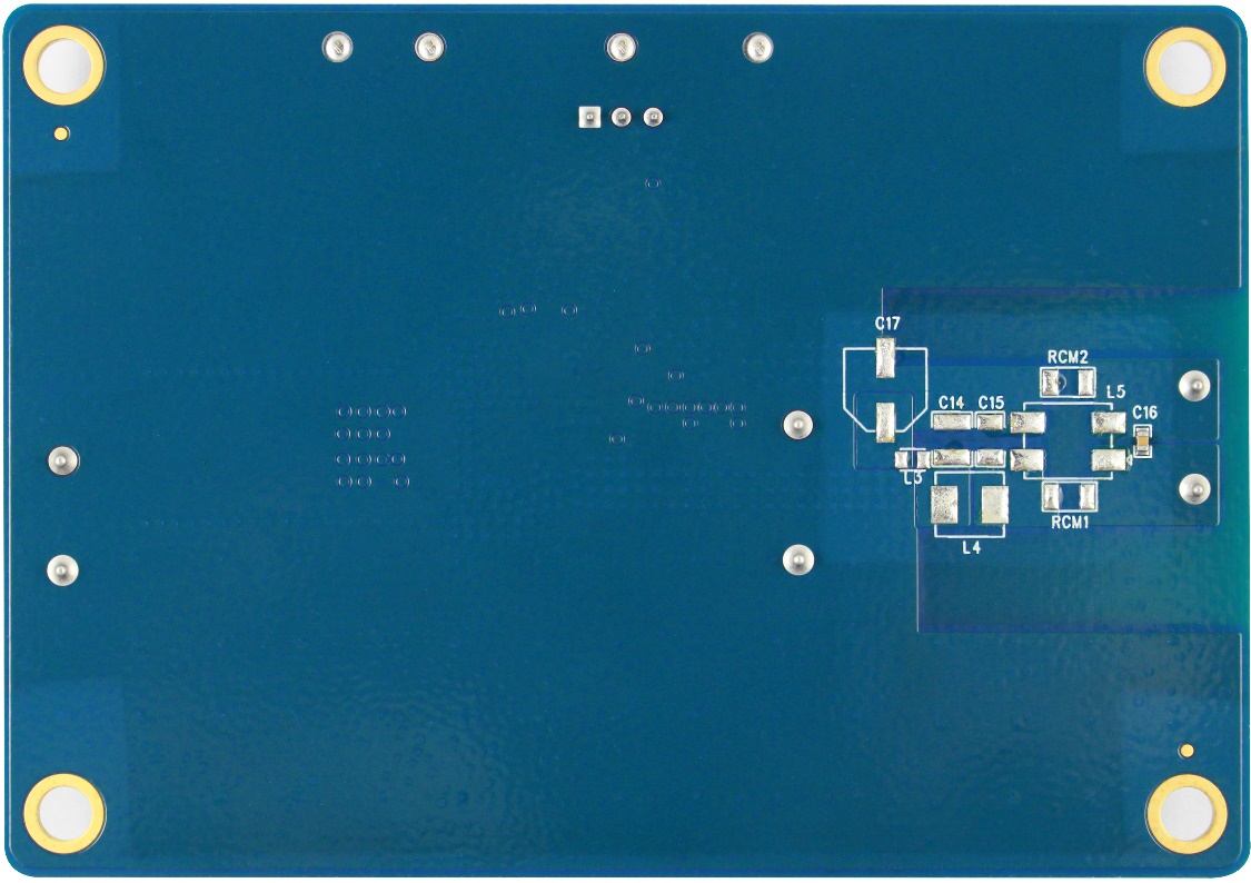
Evaluation Board Layout
Figure 1 to Figure 4 are RTQ2104GSP Evaluation Board layout. This board size is 100mm x 70mm and is constructed on four-layer PCB, outer layers with 2 oz. Cu and inner layers with 1 oz. Cu.
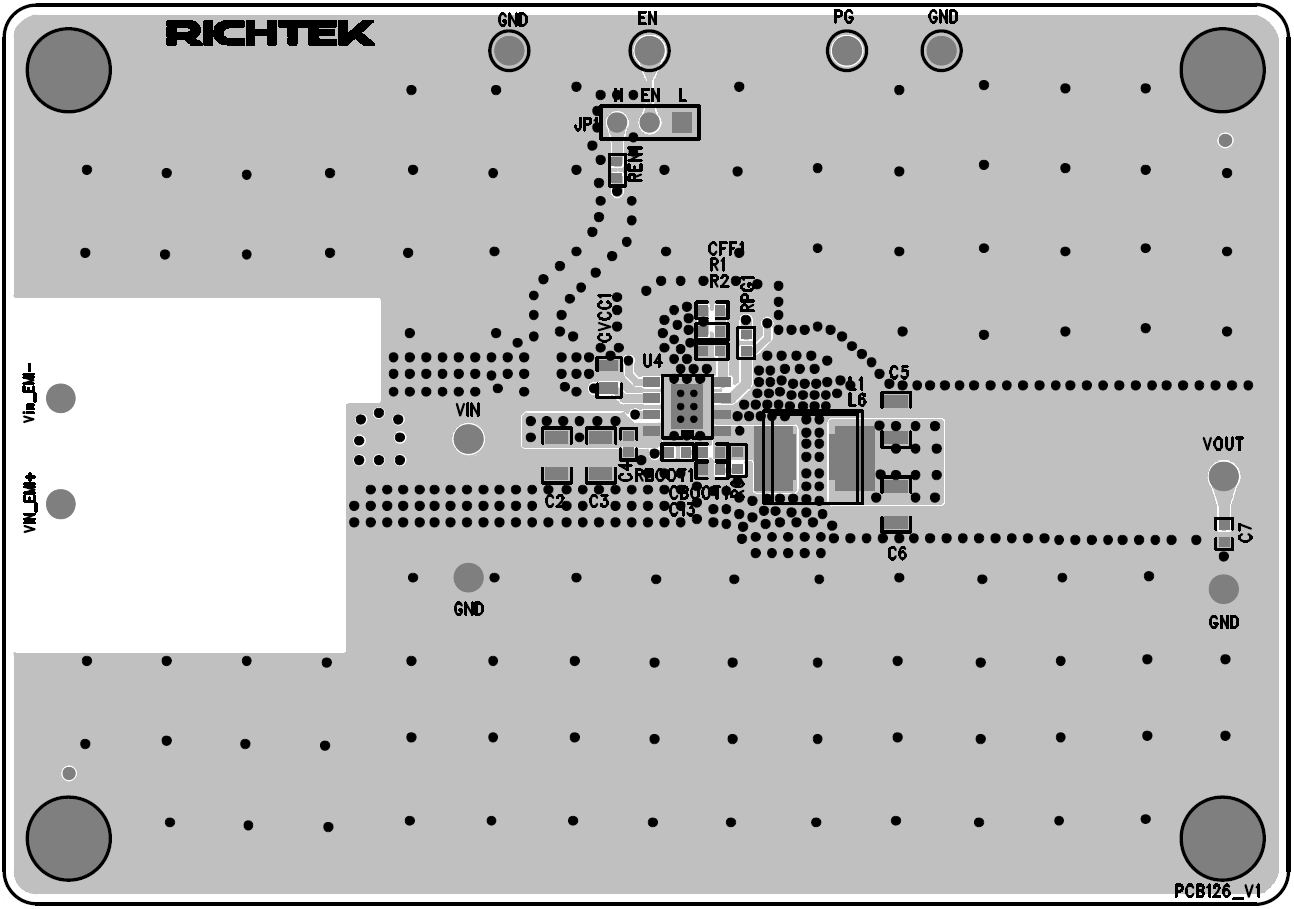
Figure 1. Top View (1st layer)
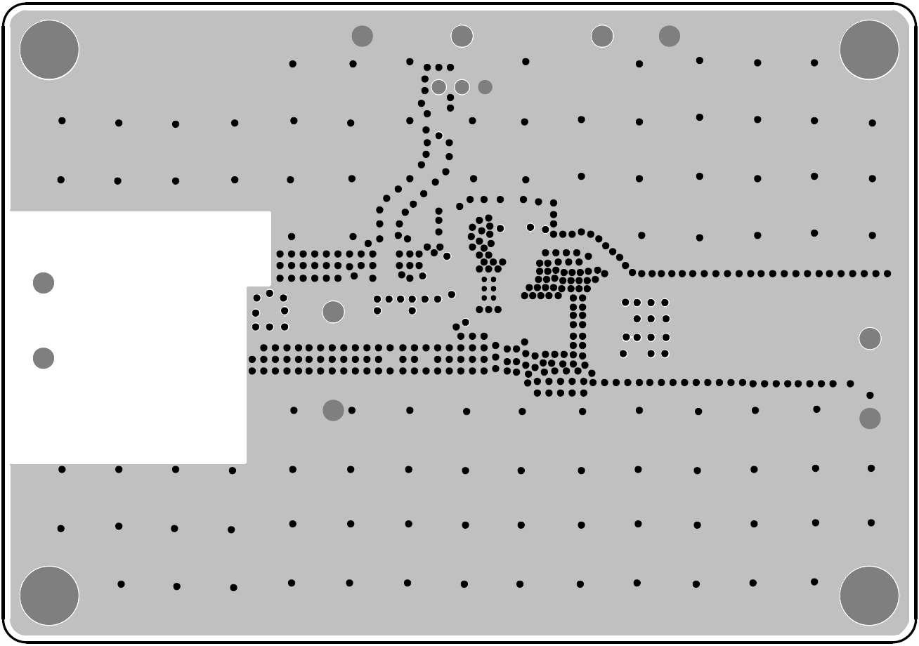
Figure 2. PCB Layout—Inner Side (2nd Layer)
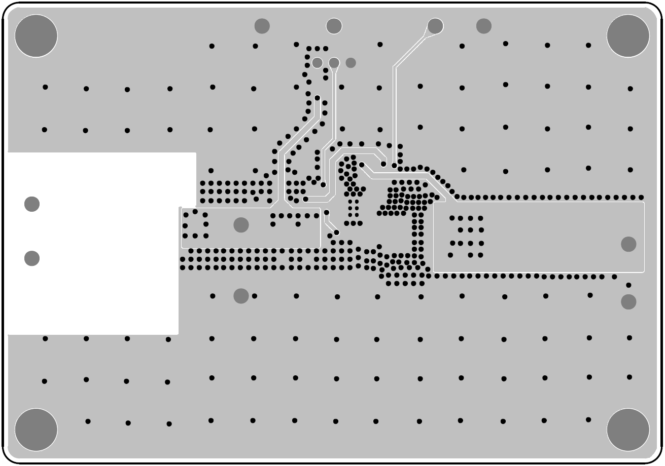
Figure 3. PCB Layout—Inner Side (3rd Layer)
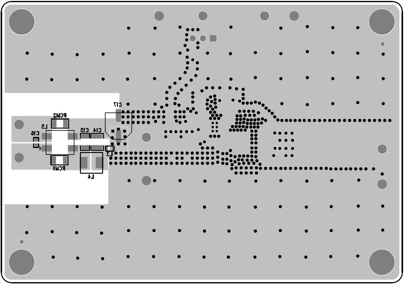
Figure 4. Bottom View (4th Layer)